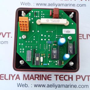
| Attribute | Value |
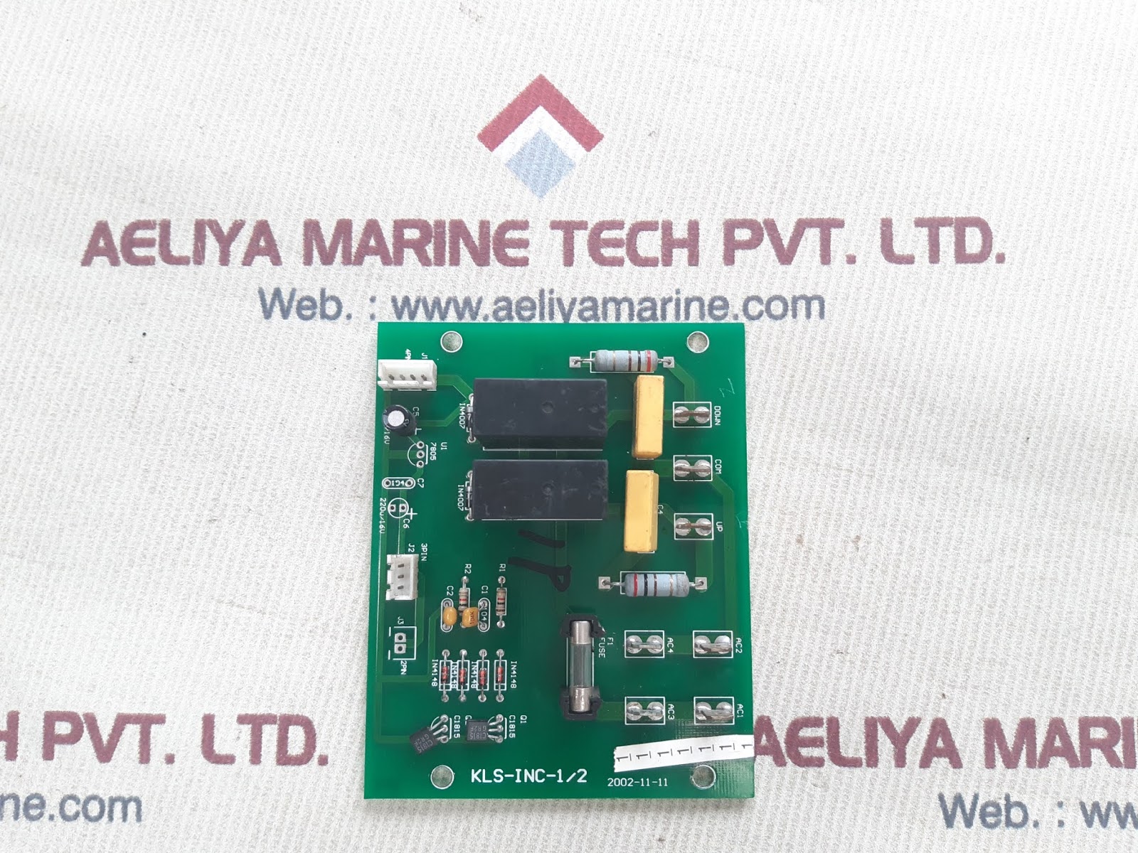
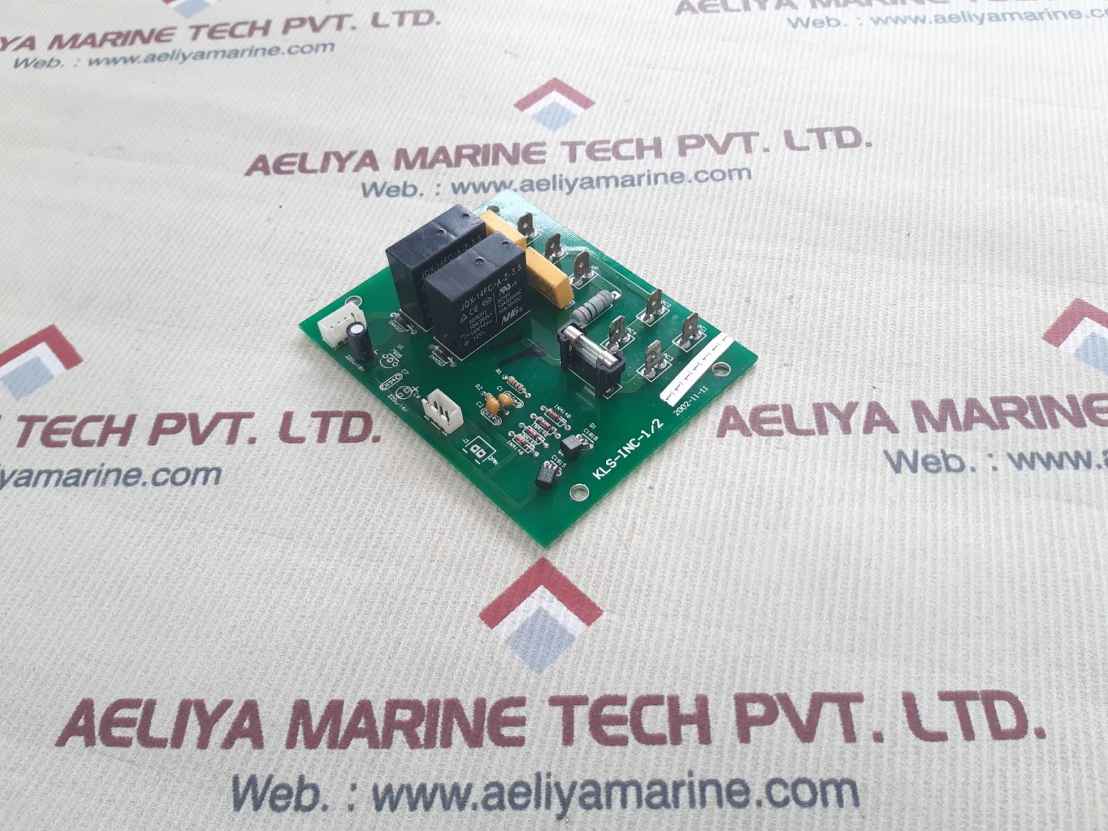
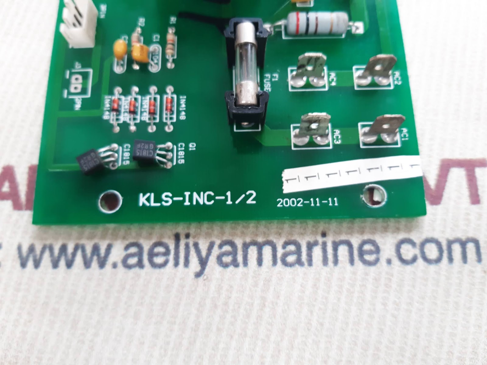
| Kls-inc-1/2 pcb card | kls-inc-1/2 |
| weight | 90gm |
Understanding the Basics
It helps to know the general purpose of PCBs before going into the details of the KLS-INC-1/2. PCBs are manufactured from a base material, which is usually fiberglass epoxy, upon which conductive paths are etched. These conductive paths, also referred to as traces, link the different electronic components mounted on the board. PCBs may be as simple as a single-layer board or as complex as a multi-layer board, depending on the complexity of the circuit.
Key Features of the KLS-INC-1/2
Although certain details regarding the KLS-INC-1/2 may only be accessed by referring to the manufacturer’s datasheet, some general features in equivalent PCB cards are discussed below:
Form Factor: The dimensions and outline of the PCB play a significant role in accommodating the target device. The “1/2” in the name may imply a half-size card, but this is subject to confirmation based on manufacturer specifications.
Layer Count: PCBs can consist of several layers of conductive traces to support more complicated circuitry. Understanding the layer count of the KLS-INC-1/2 is important in realizing its potential.
Component Mounting: The board will be engineered to hold particular types of components, like surface-mount (SMD) or through-hole components. The method of mounting impacts the production process and the number of components on the board.
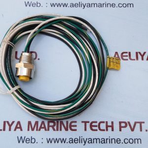
Connectivity: The KLS-INC-1/2 probably has connectors for connection to other devices or systems. These connectors may be headers, edge connectors, or other specialized interfaces.
Material: The PCB’s base material determines its thermal and electrical characteristics. FR-4 is typical, but other specialized materials may be employed based on the application.
Impedance Control: In the case of high-speed signals, impedance control of the traces is essential. The KLS-INC-1/2 may have design features to control impedance.
Surface Finish: Surface finish of the copper traces prevents them from oxidizing and ensures a good soldering surface. Typical finishes are HASL (Hot Air Solder Leveling) and ENIG (Electroless Nickel Immersion Gold).
Applications
Without knowing anything concrete about the KLS-INC-1/2, it’s hard to say exactly what it’s used for. That said, considering the general uses of PCBs, we can make some educated guesses:
Industrial Control: The card may be utilized in industrial control systems, managing equipment or processes.
Embedded Systems: The KLS-INC-1/2 may be an element of an embedded system, handling particular functions in a larger device.
Communication Devices: The card may be applied in networking hardware, telecommunications, or other communication devices.
Consumer Electronics: Although less probable with the “INC” label, perhaps the card is applied in some consumer electronics.
Advantages of Implementing the KLS-INC-1/2
Reliability: PCBs provide a reliable platform for electronic circuits to function consistently.
Compactness: PCBs provide a means of tightly packaging electronic components, keeping devices small.
Cost-Effectiveness: Mass production of PCBs renders them an economical option for the production of electronic goods.
Design Flexibility: PCBs can be designed to support a variety of circuit complexities and types of components.